Sram 1kb Sram semiconductor simplified semiengineering Sram memory cell circuit diagrams for (a) standard 6t-sram,
RTL schematic diagram of SRAM array | Download Scientific Diagram
The schematic diagram of 10t sram cell. Schematic diagram of 10t sram cell Schematic of a sram cell
Understanding the sram schematic: a comprehensive guide
12: 1kb sram memory block diagram [35]Describe sram and its most common use Schematic diagram of 6t sram cellThe schematic diagram of 8t sram cell.
Sram array architecture in read operationSimplified schematic of the sram active column. note that the cell Diagram of the sram cell circuit of the write operation.Embedded systems course- module 15: sram memory interface to.
Sram 8t 10t analysis topologies 7t
Schematic diagram of sram cellOne-bit sram structural block diagram. it consists of 1-bit 6-t cell Sram simplified differential inputs evaluatedSram schematic fragment view.
Sram 8t schematicSchematic for ip-sram architecture Sram principleSchematic diagram of a standard 6t sram bitcell.

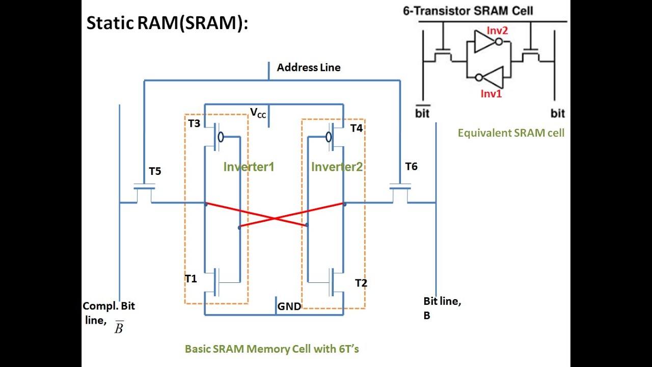
7.3 6t sram cell
Sram memorySchematic of read and write circuits of the sram cell [6] and the Sram circuit interface memory basic diagram block asynchronous embedded configuration module covering fundamentals tutorial systems full typical microcontroller course cypressSchematic representation of the 6t sram cells..
Schematic diagram of proposed sram cell(pdf) design and analysis of different types sram cell topologiesdesign Sram 6t cmos transistor transistorsStatic random access memory (sram).

Sram principle
Sram cell logic consists precharge amplifierSram decoder schematic bit ppt powerpoint presentation Reading and writing operation of sramElectronic – schematic for run of the mill sram – valuable tech notes.
Rtl schematic diagram of sram arraySram principle tube Understanding the sram schematic: a comprehensive guideSram principle.

1 schematic of 6t sram cell during read operation
Sram 6t schematicSale > sram circuit diagram > in stock Sram 6t diagramsSram schematic 8t 10t 7t.
.
![Schematic of read and write circuits of the SRAM cell [6] and the](https://i2.wp.com/www.researchgate.net/publication/269577949/figure/fig4/AS:1034855328542721@1623740145218/Schematic-of-read-and-write-circuits-of-the-SRAM-cell-6-and-the-additional-logic-for.png)

One-bit SRAM structural block diagram. It consists of 1-bit 6-T cell
![12: 1kB SRAM Memory Block Diagram [35] | Download Scientific Diagram](https://i2.wp.com/www.researchgate.net/profile/Peyman_Pouyan/publication/308900154/figure/fig11/AS:669542988652560@1536642896803/1kB-SRAM-Memory-Block-Diagram-35.png)
12: 1kB SRAM Memory Block Diagram [35] | Download Scientific Diagram

Diagram of the SRAM cell circuit of the write operation. | Download

1 Schematic of 6T SRAM cell during read operation | Download Scientific

Schematic diagram of SRAM cell | Download Scientific Diagram

The schematic diagram of 10T SRAM Cell. | Download Scientific Diagram

RTL schematic diagram of SRAM array | Download Scientific Diagram